
| Sv translation | |||||||||||||||||||||||||||||||||||||||||||||||||||||||||||||||||||||||||||||||||||||||||||||||||||||||||||||||||||||||||||||||||||||||||||||||||||||||||||||||||||||||||||||||||||||||||||||||||||||||||||||||||||||||||||||||||||||||||||||||||||||||||||||||||||||||||||||||||||||||||||||||||||||||||||||||||||||||||||||||||||||||||||||||||||||||||||||||||||||||||||||||||||||||||||||||||||||||||||||||||||||||||||||||||||||||||||||||||||||||||||||||||||||||||||||||||||||||||||||||||||||||||||||||||||||||||||||||||||||||||||||||||||||||||||||||||||||||||||||||||||||||||||||||||||||||||||||||||||||||||||||||||||||||||||||||||||||||||||||||||||||||||||||||||||||||||||||||||||||||||||
|---|---|---|---|---|---|---|---|---|---|---|---|---|---|---|---|---|---|---|---|---|---|---|---|---|---|---|---|---|---|---|---|---|---|---|---|---|---|---|---|---|---|---|---|---|---|---|---|---|---|---|---|---|---|---|---|---|---|---|---|---|---|---|---|---|---|---|---|---|---|---|---|---|---|---|---|---|---|---|---|---|---|---|---|---|---|---|---|---|---|---|---|---|---|---|---|---|---|---|---|---|---|---|---|---|---|---|---|---|---|---|---|---|---|---|---|---|---|---|---|---|---|---|---|---|---|---|---|---|---|---|---|---|---|---|---|---|---|---|---|---|---|---|---|---|---|---|---|---|---|---|---|---|---|---|---|---|---|---|---|---|---|---|---|---|---|---|---|---|---|---|---|---|---|---|---|---|---|---|---|---|---|---|---|---|---|---|---|---|---|---|---|---|---|---|---|---|---|---|---|---|---|---|---|---|---|---|---|---|---|---|---|---|---|---|---|---|---|---|---|---|---|---|---|---|---|---|---|---|---|---|---|---|---|---|---|---|---|---|---|---|---|---|---|---|---|---|---|---|---|---|---|---|---|---|---|---|---|---|---|---|---|---|---|---|---|---|---|---|---|---|---|---|---|---|---|---|---|---|---|---|---|---|---|---|---|---|---|---|---|---|---|---|---|---|---|---|---|---|---|---|---|---|---|---|---|---|---|---|---|---|---|---|---|---|---|---|---|---|---|---|---|---|---|---|---|---|---|---|---|---|---|---|---|---|---|---|---|---|---|---|---|---|---|---|---|---|---|---|---|---|---|---|---|---|---|---|---|---|---|---|---|---|---|---|---|---|---|---|---|---|---|---|---|---|---|---|---|---|---|---|---|---|---|---|---|---|---|---|---|---|---|---|---|---|---|---|---|---|---|---|---|---|---|---|---|---|---|---|---|---|---|---|---|---|---|---|---|---|---|---|---|---|---|---|---|---|---|---|---|---|---|---|---|---|---|---|---|---|---|---|---|---|---|---|---|---|---|---|---|---|---|---|---|---|---|---|---|---|---|---|---|---|---|---|---|---|---|---|---|---|---|---|---|---|---|---|---|---|---|---|---|---|---|---|---|---|---|---|---|---|---|---|---|---|---|---|---|---|---|---|---|---|---|---|---|---|---|---|---|---|---|---|---|---|---|---|---|---|---|---|---|---|---|---|---|---|---|---|---|---|---|---|---|---|---|---|---|---|---|---|---|---|---|---|---|---|---|---|---|---|---|---|---|---|---|---|---|---|---|---|---|---|---|---|---|---|---|---|---|---|---|---|---|---|---|---|---|---|---|---|---|---|---|---|---|---|---|---|---|---|---|---|---|---|---|---|---|---|---|---|---|---|---|---|---|---|---|---|---|---|---|---|---|---|---|---|---|---|---|---|---|---|---|---|---|---|---|---|---|---|---|---|---|---|---|---|---|---|---|---|---|---|---|---|---|---|---|---|---|---|---|---|---|---|---|---|---|---|---|---|---|---|---|---|---|---|---|---|---|---|---|---|---|---|---|---|---|---|---|---|---|---|---|
| |||||||||||||||||||||||||||||||||||||||||||||||||||||||||||||||||||||||||||||||||||||||||||||||||||||||||||||||||||||||||||||||||||||||||||||||||||||||||||||||||||||||||||||||||||||||||||||||||||||||||||||||||||||||||||||||||||||||||||||||||||||||||||||||||||||||||||||||||||||||||||||||||||||||||||||||||||||||||||||||||||||||||||||||||||||||||||||||||||||||||||||||||||||||||||||||||||||||||||||||||||||||||||||||||||||||||||||||||||||||||||||||||||||||||||||||||||||||||||||||||||||||||||||||||||||||||||||||||||||||||||||||||||||||||||||||||||||||||||||||||||||||||||||||||||||||||||||||||||||||||||||||||||||||||||||||||||||||||||||||||||||||||||||||||||||||||||||||||||||||||||
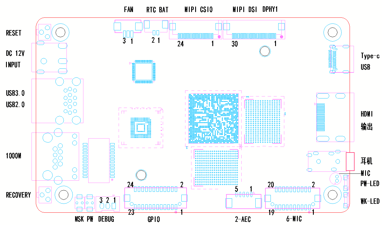
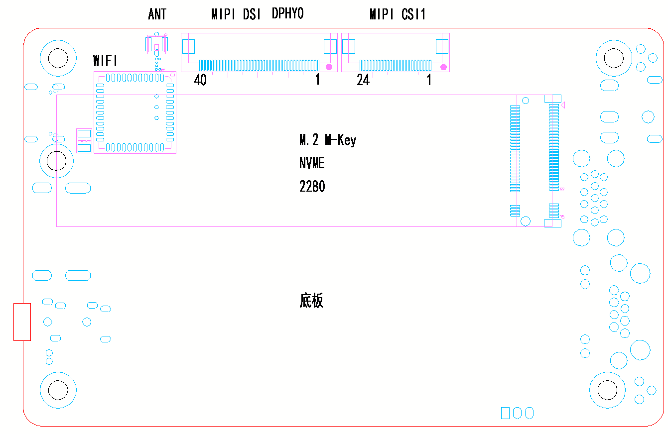
一、接口示意图
二、端口描述1.Debug 端口
2. Recovery 按键
3 .Maskrom 按键
4. Power 按键
5 .Reset 按键
6 .GPIO 端口
使用时请注意端口电平一致,电平电压不一样会损坏CPU。
7. 6-MIC 输入口6-MIC 输入口 采用的是1.25MM 2*10P 板对线 wafer 连接器,接口定义如下:
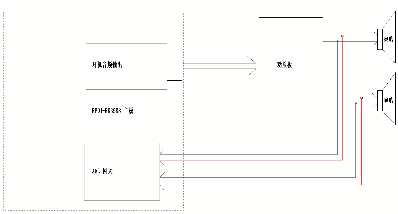
8. 2-AEC 输入端口
AEC回采 框图 | |||||||||||||||||||||||||||||||||||||||||||||||||||||||||||||||||||||||||||||||||||||||||||||||||||||||||||||||||||||||||||||||||||||||||||||||||||||||||||||||||||||||||||||||||||||||||||||||||||||||||||||||||||||||||||||||||||||||||||||||||||||||||||||||||||||||||||||||||||||||||||||||||||||||||||||||||||||||||||||||||||||||||||||||||||||||||||||||||||||||||||||||||||||||||||||||||||||||||||||||||||||||||||||||||||||||||||||||||||||||||||||||||||||||||||||||||||||||||||||||||||||||||||||||||||||||||||||||||||||||||||||||||||||||||||||||||||||||||||||||||||||||||||||||||||||||||||||||||||||||||||||||||||||||||||||||||||||||||||||||||||||||||||||||||||||||||||||||||||||||||||
RP01-RK3588S2 MIPI DSI DPHY1 Pin脚定义 | ||
Pin脚编号 | Pin 定义 | 定义说明 |
1 | GND | 电源地 |
2 | DPHY1_TX_D0N | DPHY1 数据0 负 |
3 | DPHY1_TX_D0P | DPHY1 数据0 正 |
4 | GND | 电源地 |
5 | DPHY1_TX_D1N | DPHY1 数据1 负 |
6 | DPHY1_TX_D1P | DPHY1 数据1 正 |
7 | GND | 电源地 |
8 | DPHY1_TX_CLKN | DPHY1 时钟 负 |
9 | DPHY1_TX_CLKP | DPHY1 时钟 正 |
10 | GND | 电源地 |
11 | DPHY1_TX_D2N | DPHY1 数据2 负 |
12 | DPHY1_TX_D2P | DPHY1 数据2 正 |
13 | GND | 电源地 |
14 | DPHY1_TX_D3N | DPHY1 数据3 负 |
15 | DPHY1_TX_D3P | DPHY1 数据3 正 |
16 | GND | 电源地 |
17 | MIPI_BL_PWM2 | 屏背光PWM 信号 输出 GPIO0_C4 PWM2_0 1.8V 电平 |
18 | MIPI_TE2 | 屏TE 信号输出,不用时悬空 GPIO1_B0 1.8V 电平 |
19 | LCD3V3 | 屏3.3V电源 |
20 | LCD_RST2 | 屏复位脚 输出GPIO1_B3 3.3V电平 |
21 | LCD_ID | 屏ID脚 ,默认拉低 |
22 | LCD_EN | 屏使能脚 ,默认拉高,3.3V 输出 |
23 | TP_SCL | 备用触摸 I2C SCL 3.3V电平(与DPHY0 共用) |
24 | TP_SDA | 备用触摸 I2C SDA 3.3V电平(与DPHY0 共用) |
25 | TP_INT | 备用触摸 中断输入 3.3V电平(与DPHY0 共用) |
26 | TP_RST | 备用触摸 复位输出 3.3V电平(与DPHY0 共用) |
27 | GND | 电源地 |
28-30 | LCD5V0 | 5V 电源输出 |
12. MIPI SCI0 接口
MIPI SCI0 接口采用的是0.5MM 24P FPC 连接器,连接器为上、下接,两面都可以接触。
4Lanes DPHY,每lane2.5Gbps 带宽。与CSI1组合使用 可实现8K 15FPS输入
RP01-RK3588S2 MIPI SCI0 Pin脚定义 | ||
Pin脚编号 | Pin 定义 | 定义说明 |
1 | I2C7_SDA_M0 | I2C7_SDA_M0 1.8V电平 |
2 | I2C7_SCL_M0 | I2C7_SCL_M0 1.8V电平 |
3 | GND | 电源地 |
4 | MIPI_CAM1_PDN_L | 摄像头 电源 使能 输出 GPIO3_C1 1.8V 电平 |
5 | MIPI_CAM1_RST_L | 摄像头 复位 输出 GPIO3_C1 1.8V 电平 |
6 | GND | 电源地 |
7 | MIPI_CSI0_RX_CLKN | 摄像头 CSI0 时钟 负 |
8 | MIPI_CSI0_RX_CLKP | 摄像头 CSI0 时钟 正 |
9 | GND | 电源地 |
10 | MIPI_CLKOUT | 摄像头 参考时钟输出 |
11 | GND | 电源地 |
12 | MIPI_CSI0_RX_D0N | 摄像头 CSI0 数据0 负 |
13 | MIPI_CSI0_RX_D0P | 摄像头 CSI0 数据0 正 |
14 | MIPI_CSI0_RX_D1N | 摄像头 CSI0 数据1 负 |
15 | MIPI_CSI0_RX_D1P | 摄像头 CSI0 数据1 正 |
16 | GND | 电源地 |
17 | MIPI_CSI0_RX_D2N | 摄像头 CSI0 数据2 负 |
18 | MIPI_CSI0_RX_D2P | 摄像头 CSI0 数据2 正 |
19 | MIPI_CSI0_RX_D3N | 摄像头 CSI0 数据3 负 |
20 | MIPI_CSI0_RX_D3P | 摄像头 CSI0 数据3 正 |
21 | GND | GND |
22-24 | VCC3V3 | 摄像头3.3V 输出 |
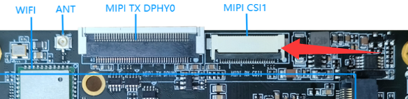
由于此板可以同时支持RK3588S和RK3588S2,区别在于MIPI RX 接口,需要在软件中调整RX链路就可以了。
链路对比如下:
| 板标识 | RK3588S | RK3588S2 | 图片 |
|---|---|---|---|
MIPI SCI0J2600 | MIPI D/C-PHY CSI_RX PORT0 1*4lane | MIPI DPHY CSI_RX PORT0 1*4lane |
|
MIPI SCI0J9906 | MIPI DPHY CSI_RX PORT0 1*4lane | MIPI DPHY CSI_RX PORT1 1*4lane |
|

13. MIPI DSI DPHY0 接口
MIPI DSI DPHY0 接口采用的是0.5MM 40P FPC 连接器,连接器为上、下接,两面都可以接触。
4Lanes DPHY,最大支持4.5Gbps 带宽。带背光输出和触摸输入。与MIPI DSI DPHY1组合使用可实现4K 分辨率输出
RP01-RK3588S2 MIPI DSI DPHY0 Pin脚定义 | ||
Pin脚编号 | Pin 定义 | 定义说明 |
1 | NC | 空脚 |
2 | VCC | 屏 3.3V电源 |
3 | IOVCC | 屏 IO电源 3.3V |
4 | GND | 电源地 |
5 | RESET | 屏复位 GPIO1_B1 3.3V电平 |
6 | NC | 空脚 |
7 | GND | 电源地 |
8 | DPHY0_TX_D0N | DPHY0 数据0 负 |
9 | DPHY0_TX_D0P | DPHY0 数据0 正 |
10 | GND | 电源地 |
11 | DPHY0_TX_D1N | DPHY0 数据1 负 |
12 | DPHY0_TX_D1P | DPHY0 数据1 正 |
13 | GND | 电源地 |
14 | DPHY0_TX_CLKN | DPHY0 时钟 负 |
15 | DPHY0_TX_CLKP | DPHY0 时钟 正 |
16 | GND | 电源地 |
17 | DPHY0_TX_D2N | DPHY0 数据2 负 |
18 | DPHY0_TX_D2P | DPHY0 数据2 正 |
19 | GND | 电源地 |
20 | DPHY0_TX_D3N | DPHY0 数据3 负 |
21 | DPHY0_TX_D3P | DPHY0 数据3 正 |
22 | GND | 电源地 |
23 | TP_VCC | 触摸电源 3.3V |
24 | TP_VCC | 触摸电源 3.3V |
25 | GND | 电源地 |
26 | TP_SDA | 触摸 I2C SDA 3.3V电平 |
27 | TP_SCL | 触摸 I2C SCL 3.3V电平 |
28 | TP_RST | 触摸 复位输出 3.3V电平 |
29 | TP_INT | 触摸 中断输入 3.3V电平 |
31-32 | LED_BL- | 屏 背光 正负,电流采样脚 |
33-38 | NC | 空脚 |
39-40 | LED_BL+ | 屏 背光 正 可输出 15-28V @50mA |
14. MIPI CSI1 接口
MIPI SCI1 接口采用的是0.5MM 24P FPC 连接器,连接器为上、下接,两面都可以接触。
4Lanes DPHY,每lane2.5Gbps 带宽。与CSI0组合使用 可实现8K 15FPS输入
RP01-RK3588S2 MIPI SCI1 Pin脚定义 | ||
Pin脚编号 | Pin 定义 | 定义说明 |
1 | I2C2_SDA_M0 | I2C2_SDA_M0 1.8V电平 |
2 | I2C2_SCL_M0 | I2C2_SCL_M0 1.8V电平 |
3 | GND | 电源地 |
4 | MIPI_CAM2_PDN_L | 摄像头 电源 使能 输出 GPIO3_C6 1.8V 电平 |
5 | MIPI_CAM2_RST_L | 摄像头 复位 输出 GPIO1_A6 1.8V 电平 |
6 | GND | 电源地 |
7 | MIPI_CSI1_RX_CLKN | 摄像头 CSI1 时钟 负 |
8 | MIPI_CSI1_RX_CLKP | 摄像头 CSI1 时钟 正 |
9 | GND | 电源地 |
10 | MIPI_CLKOUT | 摄像头 参考时钟输出 |
11 | GND | 电源地 |
12 | MIPI_CSI1_RX_D0N | 摄像头 CSI1 数据0 负 |
13 | MIPI_CSI1_RX_D0P | 摄像头 CSI1 数据0 正 |
14 | MIPI_CSI1_RX_D1N | 摄像头 CSI1 数据1 负 |
15 | MIPI_CSI1_RX_D1P | 摄像头 CSI1 数据1 正 |
16 | GND | 电源地 |
17 | MIPI_CSI1_RX_D2N | 摄像头 CSI1 数据2 负 |
18 | MIPI_CSI1_RX_D2P | 摄像头 CSI1 数据2 正 |
19 | MIPI_CSI1_RX_D3N | 摄像头 CSI1 数据3 负 |
20 | MIPI_CSI1_RX_D3P | 摄像头 CSI1 数据3 正 |
21 | GND | GND |
22-24 | VCC3V3 | 摄像头3.3V 输出 |
15. Fan 接口
风扇接口,带PWM 输出,稳定超过设定温度,自动开启。
连接器为1.25MM 3P
RP01-RK3588S2 Fan 接口 Pin脚定义 | ||
Pin脚编号 | Pin 定义 | 定义说明 |
1 | GND | 电源地 |
2 | FAN_PWM | 风扇 PWM 5V电平 |
3 | VCC_FAN | 风扇电源 默认5V输出,可以切换12V |
16. M.2 M-Key PCIE2.0
M.2 M-Key可以外接NVME SSD存储卡,2280尺寸。PCIE2.0x1lane, 5Gbps带宽。
可以兼容市场上常用的SSD存储卡。
17. 以太网
通过一个 RJ45 接口引出; 支持 10/100/1000Mbps 数据传输速率。
18. Type-c USB
支持USB3.0 OTG,可用于固件烧录,支持DP1.4a输出,最大可达4K@60Hz。
19. USB3.0&USB2.0
1 路 A型 USB3.1 Gen1 Host,数据速率高达 5Gbps;
1 路 A型 USB2.0 Host,数据速率高达 480Mbps;
双路输出电流叠加为1A。
20. HDMI输出
HDMI2.1,Type-A 连接器,最高输出8K@60Hz。
21. RTC
板载 RTC 接口,用于连接 2Pin 1.25mm 接口的 RTC 电池。
22. 电源输入接口
12V 2A 电源DC头 5.5 2.0
1
| Sv translation | |||||||||||||||||
|---|---|---|---|---|---|---|---|---|---|---|---|---|---|---|---|---|---|
| |||||||||||||||||
项目
发布日期 2026-1-28 生效日期 2026-1-28 文件状态 编修 文件拟定 王志海 文件审核 保密类型 公开 | |||||||||||||||||
版本 | 发布日期 | 升级记录 | |||||||||||||||
V1.0 | 2026-1-28 | 第一次发布 | |||||||||||||||
| Release Date | Jan. 28, 2026 |
| Effective Date | Jan. 28, 2026 |
| Document Status | Under Revision |
| Compiled by | Wang Zhihai |
| Reviewed by | |
| Confidentiality Level | Public |
| Version | Release Date | Upgrade Record |
|---|---|---|
| V1.0 | Jan. 28, 2026 | First release |
1. Interface Schematic Diagram
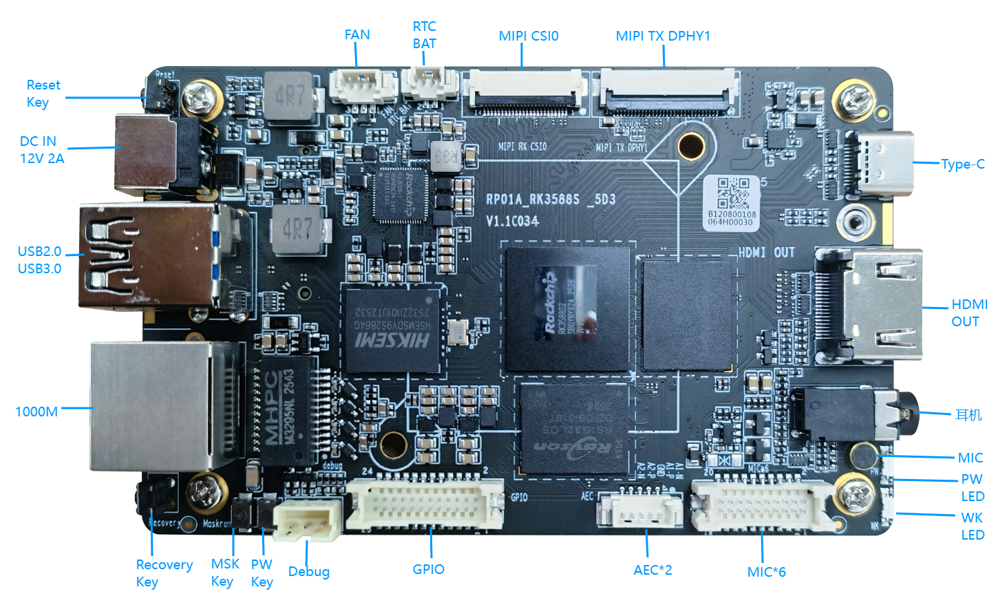


二、端口描述
2. Port Description
1. Debug
端口Port
Baud Rate: 1500000bps
Voltage Level: 3波特率:1500000bps 电平:3.3V
连接器规格 Connector Specification: 2.0MM 3P
Pin Definition of RP01-RK3588S2 Debug 端口 Pin脚定义Port | ||
Pin No.Pin脚编号 | Pin 定义Definition | 定义说明Description |
1 | RXD | 串口接收Serial Receive |
2 | TXD | 串口发送Serial Transmit |
3 | GND | 电源地Power Ground |
2. Recovery
按键Recovery按键,主要是方便系统进入 Recovery 模式,来对 EMMC 进行镜像烧录/下载。使用方法是:打开瑞芯微开发工具,断电状态下先从 Type-C OTG 口插入数据线,先摁住Recovery按键不放,然后接入12V电源,当电脑瑞芯微开发工具界面提示识别到 Recovery 设备时,即可松开按键,进行下一步的镜像烧录。
可参照固件烧录章节。
Key
The Recovery key is mainly used to enter Recovery mode for EMMC image flashing and downloading.
Operation steps: Open Rockchip Development Tool. With the power off, connect the data cable to the Type-C OTG port. Keep pressing the Recovery key, then connect the 12V power supply. Release the key once the tool detects the Recovery device, and proceed with image flashing.
Refer to the firmware flashing chapter for details.
3. Maskrom Key
The Maskrom key is used to enter MaskRom mode to flash and download images to EMMC. It is applicable for firmware corruption and system boot failure scenarios.
Operation steps: Open Rockchip Development Tool. With the power off, insert the data cable into the Type-C OTG port. Hold down the Maskrom key and connect the 12V power supply. Release the key when the tool recognizes the MaskRom device, then start image flashing.
See Chapter 5 for firmware flashing instructions.
4. Power Key
It serves as system power on/off and sleep key.
- Under Linux system: used for system power on and power off.
- Under Android system: used for system sleep function.
5. Reset Key
It is designed for system reset and reboot. Pressing this key under any status will trigger power-off restart of the system.
6. GPIO Port
Adopt 1.25MM 2*12P board-to-wafer connector. Pin definitions are listed as follows.
Note: Ensure consistent port voltage level during use. Different voltage levels may cause CPU damage.
| RP01-RK3588S2 GPIO Pin Definition | ||||||
|---|---|---|---|---|---|---|
| Pin | Voltage Level | GPIO | Function 1 | Function 2 | Function 3 | Function 4 |
3 .Maskrom 按键
MaskRom按键,主要是方便系统进入 MaskRom 模式,来对 EMMC 进行镜像烧录/下载。对于固件损坏不进系统可以按此键进行固件烧录。
使用方法是:打开瑞芯微开发工具,断电状态下先从 Type-C OTG 口插入数据线,先摁住MaskRom按键不放,然后接入12V电源,当电脑瑞芯微开发工具界面提示识别到 MaskRom 设备时,即可松开按键,进行下一步的镜像烧录。
固件烧录可参照第五章节。
4. Power 按键
主要功能是作为系统的开关机按键和休眠按键来使用。当运行的系统是 Linux 时,该按键主要用作系统开关机按键。当运行的系统是 Android 时,该按键主要用作系统休眠按键。5 .Reset 按键
主要功能是作为系统的复位重启。在任何状态下按下此键都会断电重启系统。6 .GPIO 端口
连接器是1.25MM 2*12P 板对线 wafer 连接器,接口定义如下:使用时请注意端口电平一致,电平电压不一样会损坏CPU。
| RP01-RK3588S2 GPIO Pin脚定义 | Pin | 电平 | GPIO | 功能1 | 功能2 | 功能3 | 功能4
|---|---|---|---|---|---|---|
1 | 3V3 | |||||
3 | 3V3 | |||||
5 | GND | |||||
7 | GND | |||||
9 | 3.3V | GPIO1_B7 | UART1_RX_M1 | I2C5_SDA_M3 | SPDIF1_TX_M0 | PWM13_M2 |
11 | 3.3V | GPIO1_B6 | UART1_TX_M1 | I2C5_SCL_M3 | SPDIF0_TX_M0 | MIPI_CAM1_CLK_M0 |
13 | 3.3V | GPIO1_B5 | UART7_TX_M2 | SPI0_CS1_M2 | ||
15 | 3.3V | GPIO1_B4 | UART7_RX_M2 | SPI0_CS0_M2 | ||
17 | 3.3V | GPIO4_B2 | PWM14_M1 | I2S1_SDO2 | ||
19 | 3.3V | GPIO4_B5 | PWM12_M1 | |||
21 | 3.3V | GPIO4_A3 | UART0_TX_M2 | |||
23 | 3.3V | GPIO4_A4 | UART0_RX_M2 | |||
2 | 5V0 | |||||
4 | 5V0 | |||||
6 | GND | |||||
8 | GND | |||||
10 | 3.3V | GPIO1_C1 | UART3_TX_M0 | I2C3_SCL_M0 | SPI4_MISO_M0 | |
12 | 3.3V | GPIO1_C0 | UART3_RX_M0 | I2C3_SDA_M0 | SPI4_MOSI_M0 | |
14 | PWRON_L | |||||
16 | 1.8V | GPIO1_C4 | PWM11_IR_M2 | SPI4_CS0_M0 | ||
18 | 1.8V | GPIO1_C6 | PWM15_IR_M2 | |||
20 | 1.8V | GPIO0_A4 | ||||
22 | 1.8V | GPIO0_D3 | ||||
24 | 1.8V | GPIO0_D5 | ||||
7.
6-MIC
输入口Input Port
The 6-MIC 输入口 采用的是1input port adopts 1.25MM 2*10P 板对线 wafer 连接器,接口定义如下:board-to-wire wafer connector. The interface definitions are as follows:
| RP01-RK3588S2 6- |
|---|
定义说明
Pin 定义
Pin脚编号
Pin 定义
定义说明
| MIC Input Pin Definition | |||||
|---|---|---|---|---|---|
| Pin No. | Pin Definition | Description | Pin No. | Pin Definition | Description |
| 1 | MIC1+ | ||||
| MIC1 Positive | 2 | MIC2+ |
| MIC2 Positive |
| 3 | MIC1- |
| MIC1 Negative | 4 | MIC2- |
| MIC2 Negative |
| 5 | AGND |
| Analog Ground | 6 | AGND |
| Analog Ground |
| 7 | MIC3+ |
| MIC3 Positive | 8 | MIC4+ |
| MIC4 Positive |
| 9 | MIC3- |
| MIC3 Negative | 10 | MIC4- |
| MIC4 Negative |
| 11 | AGND |
| Analog Ground | 12 | AGND |
| Analog Ground |
| 13 | MIC5+ |
| MIC5 Positive | 14 | MIC6+ |
| MIC6 Positive |
| 15 | MIC5- |
| MIC5 Negative | 16 | MIC6- |
| MIC6 Negative |
| 17 | AGND |
| Analog Ground | 18 | AGND |
| Analog Ground |
| 19 | MIC3V3 |
| MIC Power Supply | 20 | AGND |
| Analog Ground |
8. 2-AEC
输入端口Input Port
The 2-AEC 输入端口主要用于外放声音的回采,用于消除回音的采样。 连接器采用的是1input port is mainly used for external sound feedback collection to realize echo cancellation sampling. It adopts 1.25MM 1*5P 板对线 wafer 连接器,接口定义如下:board-to-wire wafer connector. The interface definitions are as follows:
| RP01-RK3588S2 2- |
|---|
| AEC Input Pin Definition | ||
|---|---|---|
| Pin No. | Pin | |
| Definition |
|---|
| Description | |
|---|---|
| 1 | AEC1_N |
| Speaker L Negative | |
| 2 | AEC1_P |
| Speaker L Positive | |
| 3 | AGND |
| Analog Ground | |
| 4 | AEC2_P |
| Speaker R Positive | |
| 5 | AEC2_N |
扬声器R负极
AEC回采 框图
9. 耳机接口
| Speaker R Negative |
AEC Echo Acquisition Block Diagram
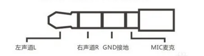
9. Headphone Interface
It integrates ES8388 audio codec, supporting audio output and microphone input. The microphone signal is connected to the IN1 channel of ES8388. It adopts standard 3.5mm 4-pole international audio jack.
Headphone Insertion Detection:HP集成ES8388 Codec,可实现声音输出和MIC输入,MIC进入ES8388 IN1 声道。接口为标准的3.5MM4节国际标准接口。
耳机插入检测:HP_DET --- GPIO1_D5---插入耳机为“1”;拔掉耳机为“0”
耳机输出开关:EAR High level "1" for headphone inserted; Low level "0" for headphone removed.
Headphone Output Control:EAR_CTL --- GPIO1_D2---输出“1”为耳机输出使能;输出“0”为耳机输出关闭.Output "1" to enable headphone output; Output "0" to disable headphone output.
10.
内置MIC内置MIC 为4020 电容式MIC,进入ES8388 IN2 声道。通过特定的算法可实现简单的语音交互。
11. MIPI DSI DPHY1 接口
MIPI DSI DPHY1 接口采用的是0.5MM 30P FPC 连接器,连接器为上、下接,两面都可以接触。4Lanes DPHY,最大支持4.5Gbps 带宽。与MIPI DSI DPHY0组合使用可实现4K 分辨率输出.
外挂转换IC,可实现MIPI转LVDS 输出。
Built-in MIC
Adopts 4020 capacitive microphone, which is connected to the IN2 channel of ES8388.
Simple voice interaction can be realized through dedicated algorithms.
11. MIPI DSI DPHY1 Interface
This interface uses 0.5MM 30P FPC connector with bidirectional contact design.
It is equipped with 4-lane DPHY, supporting maximum bandwidth up to 4.5Gbps. Combined with MIPI DSI DPHY0, it can realize 4K resolution output.
External conversion IC can be used to convert MIPI signal to LVDS output.
| RP01-RK3588S2 MIPI DSI DPHY1 |
|---|
| Pin Definition | ||
|---|---|---|
| Pin No. | Pin | |
| Definition |
|---|
| Description | |
|---|---|
| 1 | GND |
| Power Ground | ||
| 2 | DPHY1_TX_D0N | DPHY1 |
| Data 0 Negative | ||
| 3 | DPHY1_TX_D0P | DPHY1 |
| Data 0 Positive | |
| 4 | GND |
| Power Ground | ||
| 5 | DPHY1_TX_D1N | DPHY1 |
| Data 1 Negative | ||
| 6 | DPHY1_TX_D1P | DPHY1 |
| Data 1 Positive | |
| 7 | GND |
| Power Ground | ||
| 8 | DPHY1_TX_CLKN | DPHY1 |
| Clock Negative | ||
| 9 | DPHY1_TX_CLKP | DPHY1 |
| Clock Positive | |
| 10 | GND |
| Power Ground | ||
| 11 | DPHY1_TX_D2N | DPHY1 |
| Data 2 Negative | ||
| 12 | DPHY1_TX_D2P | DPHY1 |
| Data 2 Positive | |
| 13 | GND |
| Power Ground | ||
| 14 | DPHY1_TX_D3N | DPHY1 |
| Data 3 Negative | ||
| 15 | DPHY1_TX_D3P | DPHY1 |
| Data 3 Positive | |
| 16 | GND |
| Power Ground | |
| 17 | MIPI_BL_PWM2 |
| Display backlight PWM signal output, GPIO0_C4 PWM2_0, 1.8V |
| level | |
| 18 | MIPI_TE2 |
| Display TE signal output, leave floating when unused, GPIO1_B0, 1.8V |
| level | |
| 19 | LCD3V3 |
| 3.3V power supply for display | |
| 20 | LCD_RST2 |
| Display reset pin output, GPIO1_B3, 3. |
| 3V level | |
| 21 | LCD_ID |
| Display ID pin, pulled low by default | |
| 22 | LCD_EN |
| Display enable pin, pulled high by default, 3.3V |
| output | |
| 23 | TP_SCL |
| Reserved touch I2C SCL, 3. |
| 3V level (shared with DPHY0) | |
| 24 | TP_SDA |
| Reserved touch I2C SDA, 3. |
| 3V level (shared with DPHY0) | |
| 25 | TP_INT |
| Reserved touch interrupt input, 3.3V level (shared with DPHY0) | |
| 26 | TP_RST |
| Reserved touch reset output, 3.3V level (shared with DPHY0) | |
| 27 | GND |
| Power Ground | ||
| 28-30 | LCD5V0 | 5V |
12. MIPI SCI0 接口
| power output |
12. MIPI CSI0 Interface
This interface uses 0.5MM 24P FPC connector, which supports double-sided insertion.
It is configured with 4-lane DPHY, with bandwidth of 2.5Gbps per lane. When used together with CSI1, it supports 8K@15FPS video input.MIPI SCI0 接口采用的是0.5MM 24P FPC 连接器,连接器为上、下接,两面都可以接触。
4Lanes DPHY,每lane2.5Gbps 带宽。与CSI1组合使用 可实现8K 15FPS输入
| RP01-RK3588S2 MIPI |
|---|
| CSI0 Pin Definition | ||
|---|---|---|
| Pin No. | Pin | |
| Definition |
|---|
| Description | ||
|---|---|---|
| 1 | I2C7_SDA_M0 | I2C7_SDA_M0, 1. |
| 8V level | ||
| 2 | I2C7_SCL_M0 | I2C7_SCL_M0, 1. |
| 8V level | |
| 3 | GND |
| Power Ground | |
| 4 | MIPI_CAM1_PDN_L |
| Camera power enable output, GPIO3_C1, 1.8V |
| level | |
| 5 | MIPI_CAM1_RST_L |
| Camera reset output, GPIO3_C1, 1.8V |
| level | |
| 6 | GND |
| Power Ground | |
| 7 | MIPI_CSI0_RX_CLKN |
| CSI0 |
| clock negative | |
| 8 | MIPI_CSI0_RX_CLKP |
| CSI0 |
| clock positive | |
| 9 | GND |
| Power Ground | |
| 10 | MIPI_CLKOUT |
| Camera reference clock output | |
| 11 | GND |
| Power Ground | |
| 12 | MIPI_CSI0_RX_D0N |
| CSI0 |
| data 0 negative | |
| 13 | MIPI_CSI0_RX_D0P |
| CSI0 |
| data 0 positive | |
| 14 | MIPI_CSI0_RX_D1N |
| CSI0 |
| data 1 negative | |
| 15 | MIPI_CSI0_RX_D1P |
| CSI0 |
| data 1 positive | |
| 16 | GND |
| Power Ground | |
| 17 | MIPI_CSI0_RX_D2N |
| CSI0 |
| data 2 negative | |
| 18 | MIPI_CSI0_RX_D2P |
| CSI0 |
| data 2 positive | |
| 19 | MIPI_CSI0_RX_D3N |
| CSI0 |
| data 3 negative | |
| 20 | MIPI_CSI0_RX_D3P |
| CSI0 |
| data 3 positive | |
| 21 | GND |
| Ground | |
| 22-24 | VCC3V3 |
| 3.3V |
由于此板可以同时支持RK3588S和RK3588S2,区别在于MIPI RX 接口,需要在软件中调整RX链路就可以了。
链路对比如下:
| power output for camera |
Since this board is compatible with both RK3588S and RK3588S2 chips, the only difference lies in the MIPI RX interface. Users only need to adjust the RX link configuration in software.
The link comparison is shown as follows:
| Board Marking板标识 | RK3588S | RK3588S2 | 图片Picture |
|---|---|---|---|
MIPI SCI0J2600 | MIPI D/C-PHY CSI_RX PORT0 1*4lane | MIPI DPHY CSI_RX PORT0 1*4lane |
|
MIPI SCI0J9906 | MIPI DPHY CSI_RX PORT0 1*4lane | MIPI DPHY CSI_RX PORT1 1*4lane |
|
13. MIPI DSI DPHY0
接口Interface
This interface uses 0.5mm 40P FPC connector which supports double-sided connection.
It adopts 4-lane DPHY with a maximum bandwidth of 4.5Gbps, featuring backlight output and touch input functions. Combined with MIPI DSI DPHY1, it can output 4K resolution display signal.MIPI DSI DPHY0 接口采用的是0.5MM 40P FPC 连接器,连接器为上、下接,两面都可以接触。
4Lanes DPHY,最大支持4.5Gbps 带宽。带背光输出和触摸输入。与MIPI DSI DPHY1组合使用可实现4K 分辨率输出
| RP01-RK3588S2 MIPI DSI DPHY0 |
|---|
| Pin Definition | ||
|---|---|---|
| Pin No. | Pin | |
| Definition |
|---|
| Description | |
|---|---|
| 1 | NC |
| No Connection | |
| 2 | VCC |
| 3. |
| 3V power supply for display | |
| 3 | IOVCC |
| 3.3V display IO power supply | |
| 4 | GND |
| Power Ground | |
| 5 | RESET |
| Display reset, GPIO1_B1, 3. |
| 3V level | |
| 6 | NC |
| No Connection | |
| 7 | GND |
| Power Ground | ||
| 8 | DPHY0_TX_D0N | DPHY0 |
| Data 0 Negative | ||
| 9 | DPHY0_TX_D0P | DPHY0 |
| Data 0 Positive | |
| 10 | GND |
| Power Ground | ||
| 11 | DPHY0_TX_D1N | DPHY0 |
| Data 1 Negative | ||
| 12 | DPHY0_TX_D1P | DPHY0 |
| Data 1 Positive | |
| 13 | GND |
| Power Ground | ||
| 14 | DPHY0_TX_CLKN | DPHY0 |
| Clock Negative | ||
| 15 | DPHY0_TX_CLKP | DPHY0 |
| Clock Positive | |
| 16 | GND |
| Power Ground | ||
| 17 | DPHY0_TX_D2N | DPHY0 |
| Data 2 Negative | ||
| 18 | DPHY0_TX_D2P | DPHY0 |
| Data 2 Positive | |
| 19 | GND |
| Power Ground | ||
| 20 | DPHY0_TX_D3N | DPHY0 |
| Data 3 Negative | ||
| 21 | DPHY0_TX_D3P | DPHY0 |
| Data 3 Positive | |
| 22 | GND |
| Power Ground | |
| 23 | TP_VCC |
| 3.3V touch power supply | |
| 24 | TP_VCC |
| 3.3V touch power supply | |
| 25 | GND |
| Power Ground | |
| 26 | TP_SDA |
| Touch I2C SDA, 3. |
| 3V level | |
| 27 | TP_SCL |
| Touch I2C SCL, 3. |
| 3V level | |
| 28 | TP_RST |
| Touch reset output, 3. |
| 3V level | |
| 29 | TP_INT |
| Touch interrupt input, 3. |
| 3V level | |
| 31-32 | LED_BL- |
| Display backlight negative pole, current sampling pin | |
| 33-38 | NC |
| No Connection | |
| 39-40 | LED_BL+ |
| Display backlight positive pole, output 15- |
| 28V@50mA |
14. MIPI CSI1
接口Interface
This interface adopts 0.5mm 24P FPC connector with double-sided pluggable design.
It is equipped with 4-lane DPHY with 2.5Gbps bandwidth per lane. Combined with CSI0, it supports 8K@15FPS video input.MIPI SCI1 接口采用的是0.5MM 24P FPC 连接器,连接器为上、下接,两面都可以接触。
4Lanes DPHY,每lane2.5Gbps 带宽。与CSI0组合使用 可实现8K 15FPS输入
| RP01-RK3588S2 MIPI |
|---|
| CSI1 Pin Definition | ||
|---|---|---|
| Pin No. | Pin | |
| Definition |
|---|
| Description | ||
|---|---|---|
| 1 | I2C2_SDA_M0 | I2C2_SDA_M0, 1. |
| 8V level | ||
| 2 | I2C2_SCL_M0 | I2C2_SCL_M0, 1. |
| 8V level | |
| 3 | GND |
| Power Ground | |
| 4 | MIPI_CAM2_PDN_L |
| Camera power enable output, GPIO3_C6, 1.8V |
| level | |
| 5 | MIPI_CAM2_RST_L |
| Camera reset output, GPIO1_A6, 1.8V |
| level | |
| 6 | GND |
| Power Ground | |
| 7 | MIPI_CSI1_RX_CLKN |
| CSI1 |
| clock negative | |
| 8 | MIPI_CSI1_RX_CLKP |
| CSI1 |
| clock positive | |
| 9 | GND |
| Power Ground | |
| 10 | MIPI_CLKOUT |
| Camera reference clock output | |
| 11 | GND |
| Power Ground | |
| 12 | MIPI_CSI1_RX_D0N |
| CSI1 |
| data 0 negative | |
| 13 | MIPI_CSI1_RX_D0P |
| CSI1 |
| data 0 positive | |
| 14 | MIPI_CSI1_RX_D1N |
| CSI1 |
| data 1 negative | |
| 15 | MIPI_CSI1_RX_D1P |
| CSI1 |
| data 1 positive | |
| 16 | GND |
| Power Ground | |
| 17 | MIPI_CSI1_RX_D2N |
| CSI1 |
| data 2 negative | |
| 18 | MIPI_CSI1_RX_D2P |
| CSI1 |
| data 2 positive | |
| 19 | MIPI_CSI1_RX_D3N |
| CSI1 |
| data 3 negative | |
| 20 | MIPI_CSI1_RX_D3P |
| CSI1 |
| data 3 positive | |
| 21 | GND |
| Ground | |
| 22-24 | VCC3V3 |
| 3.3V |
| power output for camera |
15. Fan
接口Interface
It is a fan interface with PWM output. The fan will automatically turn on when the temperature exceeds the set threshold.
Equipped with 1.25mm 3P connector.风扇接口,带PWM 输出,稳定超过设定温度,自动开启。
连接器为1.25MM 3P
| RP01-RK3588S2 Fan |
|---|
| Interface Pin Definition | ||
|---|---|---|
| Pin No. | Pin | |
| Definition |
|---|
| Description | |
|---|---|
| 1 | GND |
| Power Ground | |
| 2 | FAN_PWM |
| Fan PWM signal, 5V level | |
| 3 | VCC_FAN |
| Fan power supply, default 5V output, switchable to 12V |
16. M.2 M-Key PCIE2.0
M.2 M-Key可以外接NVME SSD存储卡,2280尺寸。PCIE2.0x1lane, 5Gbps带宽。
可以兼容市场上常用的SSD存储卡。
17. 以太网
-Key interface supports external 2280-size NVMe SSD. Adopts PCIE2.0 x1 lane with 5Gbps bandwidth, compatible with mainstream commercial SSDs.
17. Ethernet
Led out via RJ45 connector, supports 通过一个 RJ45 接口引出; 支持 10/100/1000Mbps 数据传输速率。transmission rate.
18. Type-
cC USB
支持USB3.0 OTG,可用于固件烧录,支持DP1.4a输出,最大可达4K@60Hz。
Supports USB3.0 OTG for firmware burning, and DP1.4a video output up to 4K@60Hz.
19. USB3.0 & USB2.0
1 路 A型 USB3.1 Gen1 Host,数据速率高达 5Gbps;1 路 A型 USB2.0 Host,数据速率高达 480Mbps;
双路输出电流叠加为1A。
20. HDMI输出
HDMI2.1,Type-A 连接器,最高输出8K@60Hz。21. RTC
板载 RTC 接口,用于连接 2Pin 1.25mm 接口的 RTC 电池。
1 channel Type-A USB3.1 Gen1 Host, speed up to 5Gbps.
1 channel Type-A USB2.0 Host, speed up to 480Mbps.
Total combined output current reaches 1A.
20. HDMI Output
Adopts HDMI2.1 Type-A connector, maximum output up to 8K@60Hz.
21. RTC
Onboard RTC interface, used for connecting 2Pin 1.25mm RTC backup battery.
22. Power Input Interface
12V 2A DC power input, 5.5*2.0 standard DC jack.
22. 电源输入接口
12V 2A 电源DC头 5.5 2.0