
| Sv translation | |||||||||||||||||||||||||||||||||||||||||||||||||||||||||||||||||||||||||||||||||||||||||||||||||||||||||||||||||||||||||||||||||||||||||||||||||||||||||||||||||||||||||||||||||||||||
|---|---|---|---|---|---|---|---|---|---|---|---|---|---|---|---|---|---|---|---|---|---|---|---|---|---|---|---|---|---|---|---|---|---|---|---|---|---|---|---|---|---|---|---|---|---|---|---|---|---|---|---|---|---|---|---|---|---|---|---|---|---|---|---|---|---|---|---|---|---|---|---|---|---|---|---|---|---|---|---|---|---|---|---|---|---|---|---|---|---|---|---|---|---|---|---|---|---|---|---|---|---|---|---|---|---|---|---|---|---|---|---|---|---|---|---|---|---|---|---|---|---|---|---|---|---|---|---|---|---|---|---|---|---|---|---|---|---|---|---|---|---|---|---|---|---|---|---|---|---|---|---|---|---|---|---|---|---|---|---|---|---|---|---|---|---|---|---|---|---|---|---|---|---|---|---|---|---|---|---|---|---|---|---|
| |||||||||||||||||||||||||||||||||||||||||||||||||||||||||||||||||||||||||||||||||||||||||||||||||||||||||||||||||||||||||||||||||||||||||||||||||||||||||||||||||||||||||||||||||||||||
一、接口示意图
二、端口描述1. 电源输入接口
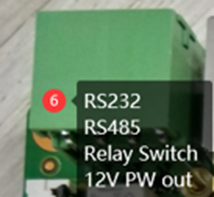
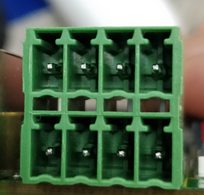
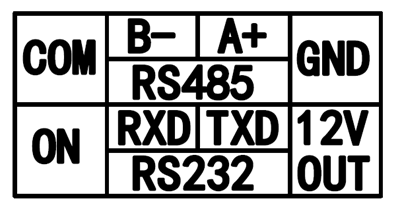
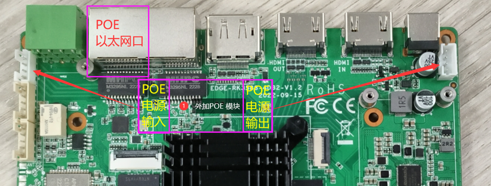
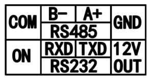
2. HDMI 输入支持 HDMI2.0 、HDMI 1.4b 输入,内置龙讯LT6911UXC HDMI2.0 支持 RGB/YCbCr4:4:4、YCbC4:2:2 2160P@30HZ; 支持 HDCP2.2 and HDCP1.4 3. HDMI 输出HDMI2.1 输出,Type-A 连接器,最高输出4K@60Hz,(安卓固件,用一个HDMI输出时,可显示8K) 支持RGB, YCbCr 4:4:4, YCbCr 4:2:2 and 8/10 bit 支持 RGB/YUV(up to 10bit) 支持HDCP2.3和DSC 1.2a 4. DP 输出DP 1.4a 输出,4Lanes 最高输出4K@60Hz。(安卓系统,单独DP 输出时,可支持8K@30HZ) 支持RGB/YUV(up to 10bit) 支持HDCP2.3, HDCP 1.3 5. 以太网*2通过一个 RJ45 接口引出; 支持 10/100/1000Mbps 数据传输速率。 网线请使用Cat5e(超五类)网线,网线长度不能超过50M,才能保证网络稳定。 避免网线由室外接入网线,室外网线容易受雷击。 6.RS232、RS485、Relay Switch 、12V PW out口RS485—ttyS0 RS232--- ttyS4 RelayControl---GPIO2_C5_d 7.POE 电源接口可以外挂POE模块,实现以太网POE供电
8-9 .备用GPIO 端口
使用时请注意端口电平一致,电平电压不一样会损坏CPU。
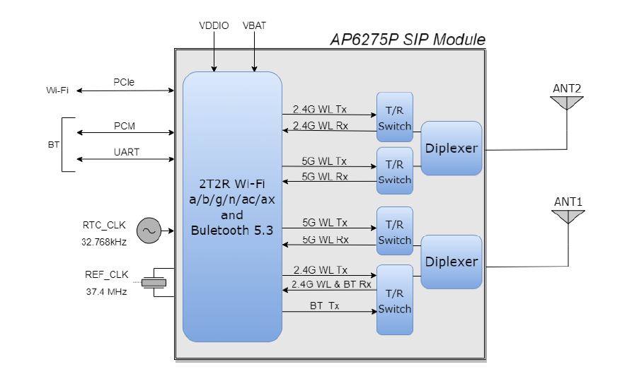
10. WIFIPCIE WIFI 6 模块,支持双发双收. 802.11a/b/g/n/ac/ax
11-12. SATA 接口SATA 3.0 接口,只支持5V 电源的硬盘或SSD。SATA为标准的7Pin SATA3.0接口。
13. M.2 PCIE 接口M.2 M-Key PCIE3.0 此接口预留80MM长的扩展卡,可扩展 SSD、边缘计算卡。为4线Pcie3.0。
15. USB3.0
16-17. USB2.0
18. Type-c USB
19 .Audio口
20. Power 按键
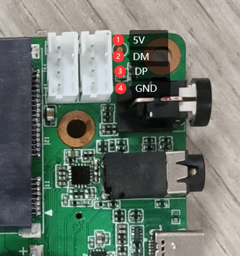
并带工作指示灯 21-22 .备用USB2.0为USB2.0 Host口,接口定义如下
| |||||||||||||||||||||||||||||||||||||||||||||||||||||||||||||||||||||||||||||||||||||||||||||||||||||||||||||||||||||||||||||||||||||||||||||||||||||||||||||||||||||||||||||||||||||||




备用端口 Pin脚定义 | ||
Pin脚编号 | Pin 定义 | 定义说明 |
1 | 12V | 12V电源输入/输出 |
2 | 12V | 12V电源输入/输出 |
3 | GND | 电源地 |
4 | GND | 电源地 |
25. Recovery 按键
Recovery按键,主要是方便系统进入 Recovery 模式,来对 EMMC 进行镜像烧录/下载。
使用方法是:打开瑞芯微开发工具,断电状态下先从 Type-C OTG 口插入数据线,先摁住Recovery按键不放,然后接入12V电源,当电脑瑞芯微开发工具界面提示识别到 Recovery 设备时,即可松开按键,进行下一步的镜像烧录。
可参照固件烧录章节。
26 .Reset 按键
主要功能是作为系统的复位重启。在任何状态下按下此键都会断电重启系统。
27.Debug 端口
波特率:1500000bps 电平:3.3V
连接器规格 2.0MM 3P
Debug 端口 Pin脚定义 | ||
Pin脚编号 | Pin 定义 | 定义说明 |
1 | RXD | 串口接收 |
2 | TXD | 串口发送 |
3 | GND | 电源地 |
28 .Maskrom 按键
MaskRom按键,主要是方便系统进入 MaskRom 模式,来对 EMMC 进行镜像烧录/下载。
对于固件损坏不进系统可以按此键进行固件烧录。
使用方法是:打开瑞芯微开发工具,断电状态下先从 Type-C OTG 口插入数据线,先摁住MaskRom按键不放,然后接入12V电源,当电脑瑞芯微开发工具界面提示识别到 MaskRom 设备时,即可松开按键,进行下一步的镜像烧录。
可参照固件烧录章节。
| Sv translation | |||||||||||||||||||||||||||||||||||||||||||||||||||||||||||||||||||||||||||||||||||||||||||||||||||||||||||||||||||||||||||||||||||||||||||||||||||||||||||||||||||||||||||||||||||||||||||||
|---|---|---|---|---|---|---|---|---|---|---|---|---|---|---|---|---|---|---|---|---|---|---|---|---|---|---|---|---|---|---|---|---|---|---|---|---|---|---|---|---|---|---|---|---|---|---|---|---|---|---|---|---|---|---|---|---|---|---|---|---|---|---|---|---|---|---|---|---|---|---|---|---|---|---|---|---|---|---|---|---|---|---|---|---|---|---|---|---|---|---|---|---|---|---|---|---|---|---|---|---|---|---|---|---|---|---|---|---|---|---|---|---|---|---|---|---|---|---|---|---|---|---|---|---|---|---|---|---|---|---|---|---|---|---|---|---|---|---|---|---|---|---|---|---|---|---|---|---|---|---|---|---|---|---|---|---|---|---|---|---|---|---|---|---|---|---|---|---|---|---|---|---|---|---|---|---|---|---|---|---|---|---|---|---|---|---|---|---|---|
| |||||||||||||||||||||||||||||||||||||||||||||||||||||||||||||||||||||||||||||||||||||||||||||||||||||||||||||||||||||||||||||||||||||||||||||||||||||||||||||||||||||||||||||||||||||||||||||
I.Interface Schematic Diagram | |||||||||||||||||||||||||||||||||||||||||||||||||||||||||||||||||||||||||||||||||||||||||||||||||||||||||||||||||||||||||||||||||||||||||||||||||||||||||||||||||||||||||||||||||||||||||||||
| Pin Definition of No.8 Spare GPIO | |||||
|---|---|---|---|---|---|
| Pin | Level | GPIO | Function 1 | Function 2 | Function 3 |
| 1 | 3.3V Power | - | - | - | - |
| 2 | GND | - | - | - | - |
| 3 | 3.3V | GPIO4_A0 | I2S1_MCLK_M0 | SPI0_MISO_M1 | Uart9_RTSN_M1 |
| 4 | 3.3V | GPIO3_D0 | I2C5_SDA_M0 | UART4_RX_M1 | PWM8_M2 |
| 5 | 3.3V | GPIO3_C6 | ISPI3_MISO_M3 | - | - |
| Pin Definition of No.9 Spare GPIO | |||||
|---|---|---|---|---|---|
| Pin | Level | GPIO | Function 1 | Function 2 | Function 3 |
| 1 | 3.3V Power | - | - | - | - |
| 2 | GND | - | - | - | - |
| 3 | 3.3V | GPIO0_C5 | I2C4_SCL_M2 | UART0_TX_M0 | PWM4_M0 |
| 4 | 3.3V | GPIO0_C4 | I2C4_SDA_M2 | UART0_RX_M0 | PWM2_M0 |
| 5 | 3.3V | GPIO3_D4 | HDMI_RX_HDPOUT | HDMI_TX_HDP_M1 | Uart9_RX_M2 |
10. Wi-Fi
PCIe Wi-Fi 6 module, 2×2 MIMO, compliant with 802.11a/b/g/n/ac/ax standards.
11-12. SATA Interface
SATA 3.0 interface, only compatible with hard drives or SSDs powered by 5V. It adopts standard 7-pin SATA 3.0 connector.
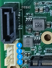
| SATA Power Port Pin Definition | ||
|---|---|---|
| Pin No. | Pin Definition | Description |
| 1 | 5V0 | SATA 5V power output |
| 2 | 5V0 | SATA 5V power output |
| 3 | GND | Power ground |
| 4 | GND | Power ground |
13. M.2 PCIe Interface
M.2 M-Key PCIe 3.0 interface, reserved for 80mm-length expansion cards. It supports expansion of SSDs and edge computing cards, featuring 4-lane PCIe 3.0.

15. USB 3.0
Type-A USB3.1 Gen1 Host interface with a maximum data rate of 5Gbps and output current of 500mA.
16-17. USB 2.0
Two Type-A USB2.0 Host ports. Maximum data rate is 480Mbps, with 500mA output current per port.
18. Type-C USB
Supports USB3.0 OTG for firmware flashing. It also features DP 1.4a output up to 4K@60Hz. (The DP function is disabled on certain firmware versions.)
19. Audio Port
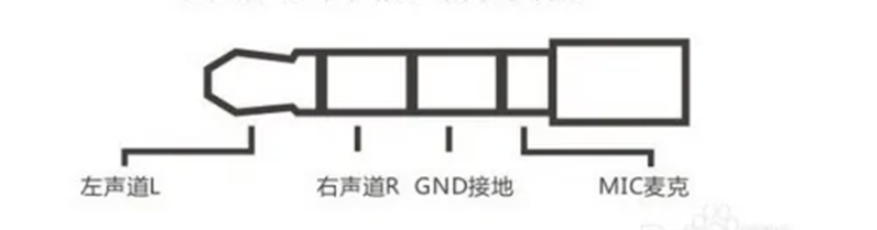
Equipped with integrated ES8323S audio codec, supporting audio output and microphone input. Adopts standard 3.5mm 4-pin TRRS connector.
20. Power Button
It serves as the power on/off and sleep button. On Linux system, it is mainly used for power control. On Android system, it functions primarily as the sleep button.
This button is equipped with a working indicator LED.
21-22. Spare USB 2.0
USB 2.0 Host ports. They adopt 2.0mm 1×4P board-to-wafer connector. The pin definition is shown below:
It serves as the power on/off and sleep button. On Linux system, it is mainly used for power control. On Android system, it functions primarily as the sleep button.This button is equipped with a working indicator LED.
| Spare Port Pin Definition | ||
|---|---|---|
| Pin No. | Pin Definition | Description |
| 1 | 5V0 | USB 5V power output |
| 2 | DM | USB data negative |
| 3 | DP | USB data positive |
| 4 | GND | Power ground |
23. 4G Module Interface
Adopts Mini PCIe connector. It supports Nano SIM card with card holder. Please select the 4G version when placing orders if 4G function is required.
24. Spare Power Interface
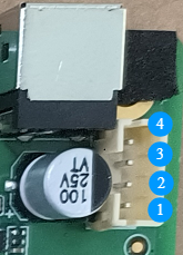
Equipped with 2.0mm 1×4P board-to-wafer connector. The pin definition is as follows:
| Spare Port Pin Definition | ||
|---|---|---|
| Pin No. | Pin Definition | Description |
| 1 | 12V | 12V power input/output |
| 2 | 12V | 12V power input/output |
| 3 | GND | Power ground |
| 4 | GND | Power ground |
25. Recovery Button
This button is used to enter Recovery mode for eMMC image flashing and downloading.
Operation steps: Launch Rockchip Development Tool. With the device powered off, connect the data cable to the Type-C OTG port. Press and hold the Recovery button, then connect the 12V power supply. Release the button once the tool detects the Recovery device, then proceed with image flashing. Refer to the firmware flashing section for details.
26. Reset Button
Used for system reset and reboot. Pressing this button will power cycle and restart the system under any operating status.
27. Debug Port
- Baud rate: 1500000 bps
- Logic level: 3.3V
- Connector: 2.0mm 3-pin
| Debug Port Pin Definition | ||
|---|---|---|
| Pin No. | Pin Definition | Description |
| 1 | RXD | Serial port receive |
| 2 | TXD | Serial port transmit |
| 3 | GND | Power ground |
28. MaskRom Button
This button is used to enter MaskRom mode for eMMC image flashing and downloading. It is applicable for firmware recovery when the device fails to boot up.
Operation steps: Launch Rockchip Development Tool. With the device powered off, connect the data cable to the Type-C OTG port. Press and hold the MaskRom button, then connect the 12V power supply. Release the button once the tool detects the MaskRom device, then proceed with image flashing. Refer to the firmware flashing section for details.